SEM
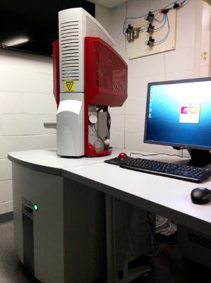
TESCAN Mira3 LMU Scanning Electron Microscope

Scanning Electron Microscopy (SEM) is a widely-used of the surface analytical technique. The primary objective of the SEM is to provide a highly magnified, highly resolved image of the surface of the specimen viewed. SEM, accompanied by X-ray analysis, is considered a relatively rapid, inexpensive, and non-destructive approach to surface analysis. It is often used to survey surface analytical problems before proceeding to techniques that are more surface-sensitive and more specialized.
The primary applications for the SEM include: materials analysis, microelectronics, earth sciences, biology, forensic science, and environmental studies
The EM Center is equipped with a TESCAN MIRA 3 LMU Variable Pressure Schottky Field Emission Scanning Electron Microscope, with a maximum resolution up to 1.2 nm at 30 kV. A new technique called environmental scanning electron microscopy (ESEM) has been engaged in the system that not only retains all the performance advantages of a conventional high vacuum SEM, but also removes the high vacuum restraint of the sample environment.
The advantages of the FESEM can be summarized as:
- Allow to mount single sample up to 100mm in diameter and 45mm thick or multiple samples
- Image of delicate samples by eliminating the need for conductive coating.
- Imaging of specimen in dynamic processes, such as tension, compression, deformation, crack propagation, adhesion, heating, cooling, freezing, melting, hydration, dehydration and sublimation
Other detectors and features of the SEM include:
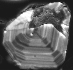
 Gatan miniCL imaging system: measures the cathodoluminescence photons in the UV, visible, near infrared and ultraviolet regime (wavelength range: 185~850 nm), which is emitted by many non-metallic materials through the interaction with electrons. The SEM-CL detector is suitable for the textures analysis of geological materials and semiconductors (e.g. quartz) that otherwise cannot be observed using optical microscopy or backscattered electrons. With biological and food specimens, CL can reveal fine scale in-homogeneity, sometime with the help of luminescent labels.
- Backscattered electron detector (BSE): measures the backscattered electron leaving the sample surface. The detector is able to provide qualitative elemental/phase information about the sample being analysed.
- Oxford Instrument INCA X-max 80mm2 EDS system: The system utilize the latest Silicon Drift Detector (SDD) technology to analyse characteristic X-rays emitted from the sample and provide semi quantitative elemental information.